
I’m a self‑driven, results‑focused professional with a broad skill set and a proven history of delivering meaningful impact. I don’t just provide solutions; I actively pursue them. When I don’t have an answer or direction, I research, test, and uncover it. My priority is helping organizations grow, perform, and succeed through competence, adaptability, and strategic execution.
Engineering, Technical Experience & Services
Phone: 661-365-5792
-
Product R&D and Product Management, Design for Manufacturing (DFM) across Consumer Electronics, Pro/Commercial environments for Audio‑Video, Security, Home Automation, LED Lighting, AC/DC Power, Wired/Wireless Networking, and IP/PoE systems. Experienced in taking hardware and software designs from proof‑of‑concept through full product launch.
-
Value‑Added Product Solutions Engineer with deep expertise in creating innovative, market‑ready solutions.
-
Electronic Engineering, Technical CAD drawings, and Consulting for product development, system architecture, and engineering documentation control/management.
-
Residential and Pro Audio/Commercial AV, Lighting, Security and Automation System Integration, including technical design, system layout, and implementation strategies for new construction projects and retrofits.
-
Creation and design of product catalogs, brochures, technical literature, instruction manuals with detailed product information/ technical specifications, packaging, website technical information/diagrams, and application notes.
-
UI/UX Design for intuitive, user‑focused interfaces across hardware and software platforms.
-
Development of technical training materials and support documentation for sales teams, trade shows, and partner education.
-
Creation of technical concepts, imagery, and presentations for customer engagement, email campaigns, LinkedIn content, training, and marketing initiatives.
-
Marketing support through technical resources, product insights, and strategic guidance to strengthen brand awareness and identify key markets and customer segments.
-
Extensive familiarity with industry leaders in AV and home automation products, systems, and technologies.
Please Note! This website is constantly in flux and a work in progress and is being updated, modified on a reqular basis.
Explore
PCB Design, Mechanical Hardware Product Example Drawings and Screenshots
'Finding Inspiration in Every Turn, empowering design excellence'
It is crucial in all product designs to thoroughly understand every aspect of project from inception to completion while ensuring that all technical and quality design requirements and expectations are met. This encompasses several key factors: 1. The physical dimensions of the PCB and the specific details of the chassis material design used for PCB integration. 2. The cost and availability of all components must align with expectations. 3. The assembly process should correspond to the established BOM costs, including parts and labor. 4. Ensuring that the components used in the design are not at End of Life (EOL) that they meet the required form, function, and technical specifications. Extensive testing processes should be conducted to evaluate the hardware and PCB for continuous operation over time. Additionally, all AC/DC voltages and Analog/Digital signals must be measured and verified for integrity, as well as checked for EMI or RF interference.


PCB Designs

PCB Designs to fit any Metal or Plastic chassis size or form factor.

Small prototype PCB runs or large OEM Production scheduled PCB deliveries.
Having the appropriate CAD, testing, and inspection tools can make significant difference. Efficient, reliable, and innovative PCBs enable engineers to design and test prior to production, reducing errors, preventing delays, and reducing costs.
PCB design and development, this includes the latest (SMT) surface mount and through hole technology (THT). I focus on achieving technical precision and implementing best practices for heat management ground planes, and effective AC/DC power routing with appropriate current management. The placement of components is essential for handling analog, digital, and RF signals, as well as for single and mixed signal PCB layouts and interactions. Careful selection of components, along with defining trace widths and signal impedance layouts, are vital aspects of the PCB design process.
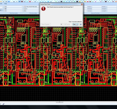
Design Verification: Netlists are essential for design rule checking (DRC) and electrical verification. By comparing the netlist with design rules and specifications, designers can detect and rectify errors such as missing connections, short circuits, or spacing requirement violations before manufacturing. process ensures the reliability and functionality of final product.
Documentation: Netlists serve as detailed records of the circuit design, encompassing component connections and pin assignments. This documentation is crucial for the design intent to team members, collaborators, or future designers who need to interpret or revise the circuit.
PCB DFM (Design for Manufacturing) Checklist
1. Material & Stack-Up
-
Use industry-standard materials (e.g., FR4)
-
Confirm layer stack-up meets impedance and thermal requirements
2. Component Placement
-
Maintain adequate spacing between components
-
Avoid placing components too close to board edges or vias
-
Group components by function to simplify routing and testing
3. Routing & Layout
-
Use consistent trace widths and spacing
-
Avoid acute angles and unnecessary vias
-
Ensure return paths for high-speed signals
4. Via Design
-
Use standard via sizes and avoid excessive via-in-pad
-
Confirm via aspect ratios are within manufacturer limits
5. Solder Mask & Silkscreen
-
Ensure proper solder mask clearance around pads
-
Avoid silkscreen on pads or vias
6. Assembly & Testability
-
Include fiducial marks for pick-and-place alignment
-
Provide test points for key signals and power rails
-
Design for automated optical inspection (AOI) and in-circuit testing (ICT)
7. Panel Layout Strategy & Mechanical
-
Add tooling holes and breakaway tabs if needed
-
Ensure board outline and cutouts are clearly defined


40-101R Rear View
100 Channel QAM HDMI Receiver PCB Layout. Product brochure, Click Here
-
Detailed CAD drawings showing all PCB layout footprints and physical locations and designators of Components.
-
DC Input for Power Connectivity
-
RF Signal L.E.D. and RF Input/Output Signal Jacks
-
IR Input/ Output Jacks, USB Jack
-
Front Panel Buttons, Controls, L.E.D. Displays/Indicators and details that are relevant to the PCB product design.
Explore
Mechanical Designs
Good designs are based on excellent concepts and properly designed details using best practices. Create designs that are explicitly simple.
Defining Problems and Functional requirements for the project. Selecting appropriate Materials and Manufacturing processes. Managing proper materials, Aluminum, Steel, Plastics related to the technology being designed and used making sure RF, EMI signals are properly addressed.


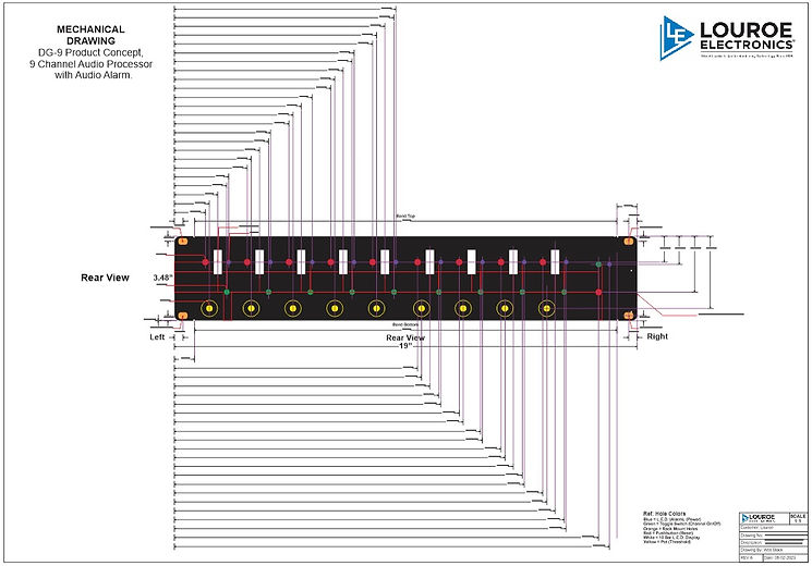
Ref: (Mechanical Diagram Rear View) DG-9 Product Concept, 9 Channel Audio Processor with Audio Alarm.
-
Creation of Detailed Technical CAD drawings showing all Physical Details, Assembly Design, with Panel/Chassis Hole Cutout References.
Ref: (Mechanical Diagram Front, Side Panel views) DG-9 Product Concept, 9 Channel Audio Processor with Audio Alarm.

-
Creation of Detailed CAD drawings showing Front, Top and Bottom side bend panel profiles.
Ref: (Mechanical+Silkscreen Layout Diagram) DG-9 Product Concept, 9 Channel Audio Processor with Audio Alarm.

-
Creation of Detailed CAD drawings showing all Silkscreen Text and operational outline references.
Ref: (Aluminum Material Front Panel Layout Diagram) Digital IP Microphone.
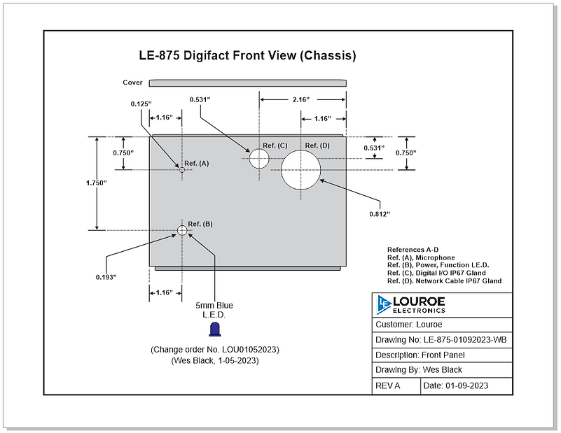
-
Digital IP Microphone CAD drawing showing Aluminum Chassis Front Panel Hole Cutouts.
Click Here to open the PDF document.